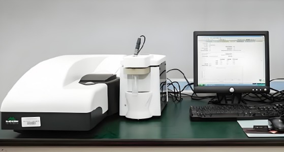
Wafer plasma etching testing is a critical process validation and quality control procedure in semiconductor manufacturing, used to evaluate etch rate, uniformity, selectivity, and profile control on silicon, dielectric, and compound semiconductor wafers. Accredited third-party laboratories perform these evaluations in accordance with SEMI, ISO, ASTM, and IEC standards to support process development, yield improvement, and failure analysis. This article provides a comprehensive technical overview of wafer plasma etching testing, including sample types, test items, methodologies, and industry applications.
Technical Overview
Wafer plasma etching testing, also referred to as plasma dry etching or plasma corrosion testing, is the systematic characterization of plasma-based material removal processes applied to semiconductor wafers. In plasma etching, a radio-frequency (RF) discharge ionizes process gases such as CF4, SF6, Cl2, BCl3, CHF3, or O2, generating chemically reactive radicals and energetic ions that remove exposed material through both chemical reactions and physical ion bombardment. Because plasma etching offers high selectivity, anisotropic profiles, and precise dimensional control, it is the dominant pattern-transfer technique in modern integrated circuit, MEMS, and photonic device manufacturing.
Testing is essential because plasma processes are highly sensitive to chamber conditions, gas chemistry, pressure, power, and wafer loading. Small deviations can cause non-uniform etching, loss of critical dimension (CD), unwanted substrate damage, or post-etch corrosion caused by residual halogen species. Accredited third-party laboratories operating under ISO/IEC 17025 quality systems conduct wafer plasma etching tests to:
- Quantify etch rate, uniformity, and selectivity for process window definition
- Verify anisotropy, sidewall angle, and profile quality
- Detect plasma-induced damage and post-etch corrosion mechanisms
- Qualify new films, masks, gases, and hardware configurations
- Support failure analysis and yield improvement programs
Testing is typically performed in ISO 14644-1 controlled cleanroom environments, with measurement methods aligned to SEMI material and metrology standards, ASTM surface-analysis practices, IEC test method conventions, and relevant JIS specifications for wafer surface inspection.
Testing Samples
Bare Silicon and Polysilicon Wafers
Monitor wafers of monocrystalline silicon, polysilicon, and silicon-on-insulator (SOI) substrates are used to evaluate baseline silicon etch behavior. These samples, typically 100 mm to 300 mm in diameter and compliant with SEMI M1 specifications, allow etch rate and uniformity mapping across the full wafer surface.
Dielectric Film Wafers
Wafers coated with silicon dioxide, silicon nitride, low-k dielectrics, or high-k oxides are tested to determine etch rates and film-to-mask selectivity. Dielectric etch characterization is essential for contact, via, and trench formation in advanced interconnect structures.
Compound Semiconductor Wafers
Gallium arsenide (GaAs), indium phosphide (InP), gallium nitride (GaN), and silicon carbide (SiC) wafers are evaluated for specialized etch chemistries. Chlorine- and methane-hydrogen-based plasmas are commonly tested for III-V materials, while fluorine-based processes are characterized for wide-bandgap substrates used in RF and power devices.
Metal and Barrier Layer Wafers
Wafers with aluminum, tungsten, titanium, titanium nitride, tantalum nitride, or copper layers are tested for metal etch performance and post-etch corrosion resistance. Chlorine-based metal etching is particularly prone to residual chlorine corrosion, making corrosion evaluation a key test focus.
Patterned Wafers with Photoresist Masks
Product-like patterned wafers or lithographically defined test vehicles are etched to assess real pattern-transfer performance, including CD bias, microloading effects, mask selectivity, and profile fidelity across varying feature densities.
MEMS and Advanced Packaging Wafers
Deep silicon etch testing is performed on MEMS wafers, through-silicon via (TSV) substrates, and 3D integration structures to validate high-aspect-ratio etching, scallop control, and depth uniformity.
Testing Items
Wafer plasma etching test programs are tailored to the material system and application, and typically include the following characterization items:
- Etch rate determination, expressed in angstroms or nanometers per minute
- Within-wafer (WIW) and wafer-to-wafer (WTW) etch uniformity mapping
- Etch selectivity of film to mask and film to substrate
- Sidewall angle and anisotropy index measurement
- Critical dimension (CD) bias, CD uniformity, and mask CD loss
- Microloading and macro-loading effect evaluation
- Etch depth, aspect ratio capability, and scallop size for deep etch processes
- Post-etch surface roughness and micromasking assessment
- Residual polymer, halogen residue, and surface contamination analysis
- Plasma-induced damage evaluation, including charging and lattice damage
- Post-etch corrosion susceptibility testing of metal layers
- Endpoint detection behavior and over-etch tolerance characterization
Each test item is documented with full process recipes, metrology data, and statistical analysis, providing clients with actionable data for process transfer or optimization.
Testing Methods
Reactive Ion Etching (RIE) Test Protocol
Conventional RIE testing uses a capacitively coupled plasma at pressures between 10 mTorr and 500 mTorr. The wafer is placed on a powered electrode, generating directional ion bombardment. Test engineers execute designed experiments varying RF power, pressure, gas flow ratios, and temperature, then measure the resulting etch responses using standardized metrology.
Inductively Coupled Plasma (ICP) Etching Test Protocol
ICP testing decouples plasma generation from ion acceleration using independent coil and platen power sources, achieving high plasma density with independently controllable ion energy. This method is used for high-rate, low-damage etch characterization of dielectrics, compound semiconductors, and metals.
Deep Reactive Ion Etching (DRIE) Testing
DRIE testing evaluates the Bosch process, which alternates SF6 etch steps with C4F8 passivation steps, and cryogenic etch variants. Testing focuses on etch depth, verticality, scallop dimension, aspect-ratio-dependent etching, and depth uniformity for MEMS and TSV applications.
Post-Etch Metrology and Characterization
Comprehensive analytical methods are applied before and after plasma exposure:
- Stylus profilometry and optical interferometry for etch depth and step height
- Spectroscopic ellipsometry and reflectometry for film thickness loss
- Scanning electron microscopy (SEM) for CD, profile, and cross-sectional analysis
- Atomic force microscopy (AFM) for post-etch surface roughness
- X-ray photoelectron spectroscopy (XPS) for surface chemistry and residue identification
- Transmission electron microscopy (TEM) for lattice damage and interfacial analysis
- Electrical and contact-angle testing for plasma-induced damage and surface energy changes
- Environmental exposure testing for post-etch corrosion evaluation of halogen-etched metals
All procedures follow documented quality protocols consistent with SEMI metrology guidance, ASTM surface analysis practices, and IEC test documentation conventions, and are performed by accredited third-party laboratories under ISO/IEC 17025 accredited management systems.
Applications
Wafer plasma etching testing services support a broad range of industries and development activities:
- Logic and memory integrated circuit process development and transfer
- MEMS sensor and actuator fabrication, including inertial, pressure, and microfluidic devices
- RF and power semiconductor manufacturing on GaN and SiC substrates
- Photonic and optoelectronic device production, including lasers and waveguides
- Advanced packaging with through-silicon vias, redistribution layers, and wafer-level bonding
- Thin-film and display processing on glass or flexible carriers
- Incoming material qualification for wafer fabrication facilities
- Failure analysis, root-cause investigation, and yield enhancement studies
- Research and development for universities, institutes, and emerging technology companies
FAQ
What is wafer plasma etching testing?
It is a laboratory evaluation of plasma dry etch processes on semiconductor wafers, measuring parameters such as etch rate, uniformity, selectivity, profile, and damage in order to validate or optimize manufacturing processes.
What wafer sizes and materials can be tested?
Accredited third-party laboratories typically accept wafers from 50 mm to 300 mm in diameter, including silicon, SOI, dielectric-coated, metal-coated, patterned, and compound semiconductor wafers such as GaAs, GaN, SiC, and InP.
How is etch rate measured during testing?
Eth rate is determined by comparing film thickness or step height before and after plasma exposure, using profilometry, ellipsometry, or reflectometry, with results reported in angstroms or nanometers per minute.
What is the difference between isotropic and anisotropic etching?
Isotropic etching removes material equally in all directions, producing rounded profiles, while anisotropic etching removes material predominantly in the vertical direction, producing vertical sidewalls required for accurate pattern transfer in advanced devices.
Why is post-etch corrosion testing important?
Chlorine-based plasma etching of metals such as aluminum can leave residual chlorine that reacts with ambient moisture and causes delayed corrosion. Corrosion testing verifies post-etch passivation and rinsing effectiveness, protecting device reliability.
How long does a typical test take?
Standard etch rate and uniformity evaluations are usually completed within three to seven working days. Complex programs involving design-of-experiments, cross-sectional SEM, or surface chemistry analysis may require additional time, and exact schedules are confirmed by the laboratory based on scope.
Can product wafers be tested without destruction?
Yes. Non-destructive metrology such as ellipsometry, optical profilometry, and CD-SEM can be applied directly to product wafers. Where cross-sectioning or TEM is required, laboratories typically use designated monitor wafers or sacrificial die to preserve valuable product material.
What standards govern wafer plasma etching testing?
Testing is conducted with reference to SEMI wafer material and metrology standards, ISO 14644 cleanroom classifications, ISO/IEC 17025 laboratory competence requirements, ASTM surface analysis practices, IEC test method conventions, and applicable JIS surface inspection specifications.