TEM Testing Service – Accredited Transmission Electron Microscopy for Ultra‑Structural Analysis in Global Markets
Our internationally accredited laboratory provides a specialist TEM testing service that empowers materials scientists, semiconductor developers, pharmaceutical researchers, metallurgists, polymer engineers and nanotechnology innovators worldwide with the highest‑resolution imaging, diffraction and microanalytical data commercially available. Every investigation is conducted within the rigorous framework of ISO/IEC 17025, and each report bearing the ILAC mark is unconditionally accepted by regulatory authorities, customs offices and notified bodies in all major economies. The TEM testing service utilises a field‑emission transmission electron microscope operating at accelerating voltages up to 300 kV, enabling atomic‑scale resolution imaging, selected‑area electron diffraction, high‑angle annular dark‑field scanning‑transmission electron microscopy and energy‑dispersive X‑ray spectroscopy. For a semiconductor foundry characterising the thickness and composition of a gate oxide, a pharmaceutical company investigating the morphology of a poorly soluble drug nanocrystal, or a steel producer analysing nanometre‑sized precipitates in a high‑strength alloy, our platform generates the legally robust, defensible microstructural evidence that supports product qualification, patent litigation and international regulatory submissions.
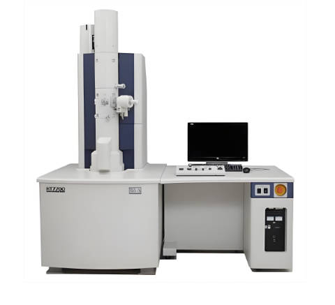
Product Samples We Regularly Subject to TEM Testing
The specimen‑preparation laboratory adjoining our TEM suite is equipped with focused‑ion‑beam milling, cryo‑ultramicrotomy, precision ion‑polishing and electropolishing systems, enabling the preparation of electron‑transparent lamellae from almost any solid material. The following categories represent the samples most frequently analysed through our TEM testing service:
- Semiconductor and electronic materials – silicon wafers, gate stacks, epitaxial layers, quantum wells, metallisation lines, solder bumps and failure‑analysis lamellae cut from specific device locations
- Metals and alloys – precipitates in aluminium, titanium and nickel‑base alloys, grain‑boundary phases, dislocation structures, martensite laths and nanometre‑sized intermetallic compounds
- Ceramics, glasses and advanced inorganic materials – zirconia‑toughened ceramics, perovskite solar‑cell layers, ferroelectric domains, catalyst nanoparticles and battery‑electrode particles
- Polymers, composites and soft materials – block‑copolymer morphologies, nanofiller dispersion in polymers, core‑shell latex particles, nanofibres and microphase‑separated structures
- Pharmaceuticals and biopharmaceuticals – nanocrystalline drug particles, liposomes, lipid nanoparticles, virus‑like particles, protein aggregates and vaccine adjuvants
- Natural and environmental nanomaterials – clay mineral platelets, natural organic‑matter colloids, airborne ultrafine particles and microplastic fragments
- Forensic and failure‑analysis samples – wear debris, corrosion‑product layers, paint cross‑sections, questioned pigment particles and counterfeit‑product residues
High‑Resolution Imaging and Electron Diffraction – TEM Testing Service for Nanostructure and Phase Identification
- Atomic‑resolution lattice‑fringe imaging and high‑resolution TEM according to the principles of ASTM E2903 and ISO 29301: the specimen is oriented along a low‑index zone axis, and a phase‑contrast image is recorded with a parallel electron beam. The lattice spacing, the symmetry of the atomic arrangement and the presence of defects such as dislocations, stacking faults and twin boundaries are determined. This TEM testing service provides the direct visual evidence of the crystal structure that is essential for the identification of polymorphs, the characterisation of epitaxial relationships and the investigation of interface quality in semiconductor devices.
- Selected‑area electron diffraction and nano‑beam diffraction for phase identification and orientation analysis: a selected region of the specimen is illuminated with a parallel beam, and the resulting diffraction pattern is recorded on a CCD or CMOS camera. The interplanar spacings and the angles between reflections are measured and compared with crystallographic databases, enabling the unambiguous identification of the crystalline phases present, even when they are present as sub‑micrometre inclusions or grain‑boundary precipitates.
- Scanning‑transmission electron microscopy imaging with high‑angle annular dark‑field and bright‑field detectors: the electron beam is focused to a sub‑angström probe and raster‑scanned across the specimen. The high‑angle annular dark‑field image, in which the intensity is approximately proportional to the square of the atomic number, reveals compositional variations at the atomic scale without the phase‑contrast artefacts that can complicate conventional HRTEM interpretation. This technique is widely used for the characterisation of quantum‑dot structures, core‑shell catalysts and the atomic‑scale chemical ordering in alloys.
- Cryo‑TEM for the analysis of beam‑sensitive and hydrated specimens: the sample is plunge‑frozen in liquid ethane and transferred into the microscope under cryogenic conditions, preserving the native hydrated state of the material. Lipid nanoparticles, liposomes, virus‑like particles, protein aggregates and other biological or soft‑matter assemblies are imaged without staining or dehydration artefacts, providing the regulatory‑grade characterisation data required for liposomal and nanoparticle‑based drug products.
- Electron energy‑loss spectroscopy for light‑element detection and chemical‑state analysis: the energy lost by the primary electrons as they pass through the specimen is analysed, revealing the elemental composition – including lithium, boron, carbon, nitrogen and oxygen – with sub‑nanometre spatial resolution. The technique also provides information on the chemical bonding and the oxidation state of the absorbing atoms, directly supporting the development of battery materials, graphene‑based devices and advanced dielectrics.
Energy‑Dispersive X‑ray Spectroscopy in the TEM – Elemental Microanalysis with Nanometre Resolution
- Quantitative elemental analysis and elemental mapping by STEM‑EDS according to the principles of ISO 22309 and ASTM E1508: the focused electron beam is positioned on a precipitate, an inclusion, a grain‑boundary phase or a layered structure, and the characteristic X‑rays are detected by a windowless silicon‑drift detector. The composition is determined from the intensities of the X‑ray lines using the Cliff‑Lorimer method or the ζ‑factor correction, and the results are reported in weight percent or atomic percent. This TEM testing service identifies the chemical identity of nanometre‑sized features that are far below the spatial resolution of scanning‑electron‑microscope‑based EDS.
- Elemental line‑scans and two‑dimensional compositional maps across interfaces: the beam is stepped across a grain boundary, a diffusion couple, an oxidation layer or a semiconductor heterostructure, and the concentration of each element is plotted as a function of position. The width of the interdiffusion zone, the segregation of impurity elements to the boundary and the abruptness of an epitaxial interface are quantified with sub‑nanometre precision.
- Quantification of light elements in battery materials, catalysts and advanced ceramics: the windowless detector and the thin‑specimen geometry enable the detection and quantification of lithium, boron, carbon, nitrogen, oxygen and fluorine, which are critical elements in lithium‑ion battery cathodes and anodes, solid‑electrolyte interphases, fuel‑cell catalysts and oxidation‑resistant coatings. The data are used by research and development teams worldwide to correlate the electrochemical performance with the local composition and to guide the synthesis of new materials.
- Precipitate and inclusion characterisation in metals and alloys: the size, shape, crystallography and elemental composition of carbides, nitrides, carbonitrides, intermetallic phases and non‑metallic inclusions are determined by a combination of imaging, diffraction and EDS. The results support the qualification of heat‑treatment procedures, the investigation of premature failures and the reverse‑engineering of competitive alloys.
Report Acceptance and Global Regulatory Compliance
All investigations performed within our TEM testing service are executed under the fully accredited scope of our ISO/IEC 17025 quality management system. Each test report that carries the ILAC mark is therefore automatically recognised by regulatory authorities, notified bodies, customs offices and supply‑chain partners in all major economies. For semiconductor manufacturers, pharmaceutical developers, metallurgical processors and advanced‑materials companies anywhere in the world, the report constitutes legally robust, internationally accepted evidence that the nanostructural characterisation, the phase identification and the elemental microanalysis have been performed in accordance with the applicable ASTM, ISO and customer‑specified methods. The documentation can be directly used for product registration, failure‑analysis reports, patent‑litigation support, the issue of inspection certificates according to EN 10204 or equivalent national standards, and the resolution of commercial and technical disputes concerning the microstructure and composition of any material at the nanometre scale.