STM Testing Service – Accredited Atomic‑Scale Surface Imaging and Electronic Characterisation for Global Markets
Our internationally accredited laboratory provides a specialist STM testing service that delivers atomic‑resolution surface topography, local electronic density‑of‑states measurements and molecular‑scale manipulation data for researchers, semiconductor developers, nanotechnology companies, catalyst producers and advanced‑materials scientists worldwide. Every measurement is performed within the rigorous framework of ISO/IEC 17025, and each report bearing the ILAC mark is unconditionally accepted by regulatory authorities, research funding bodies and supply‑chain partners in all major economies. The STM testing service exploits the quantum‑mechanical tunnelling current between an atomically sharp probe tip and a conductive or semi‑conductive surface to map individual atoms, measure the local work function, acquire scanning tunnelling spectra and probe the electronic structure of nanostructures with an energy resolution that approaches the thermal limit. By operating in ultra‑high vacuum, ambient and controlled‑gas environments, and by combining the STM with low‑temperature stages, our platform gives clients the legally robust, defensible data required to understand the atomic‑scale structure–property relationships that govern catalytic activity, corrosion resistance, molecular‑electronics performance and quantum‑device behaviour.
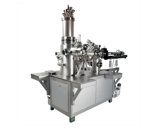
Product Samples We Regularly Subject to STM Testing
The sample‑mounting stages and the tip‑preparation facilities of our STM laboratory accept a broad variety of flat, conductive or semi‑conductive specimens. The following categories represent the materials most frequently analysed through our STM testing service:
- Semiconductor surfaces and heterostructures – silicon (111)‑7×7, gallium arsenide, indium phosphide, silicon carbide, monolayer and few‑layer transition‑metal dichalcogenides and III‑V quantum‑well cleaved edges
- Metallic and bimetallic surfaces – gold (111), silver (111), platinum (111), copper (111), palladium, nickel and ultra‑thin metal films on oxide or graphite supports
- Carbon‑based nanomaterials – highly oriented pyrolytic graphite, graphene on silicon carbide or metal substrates, carbon nanotubes and fullerenes
- Functional organic molecules and self‑assembled monolayers – porphyrins, phthalocyanines, alkanethiols, DNA bases and molecular switches deposited on conductive substrates
- Catalysts and electrocatalysts – oxide‑supported metal nanoparticles, perovskite oxide surfaces, ex‑solved metal particles on ceramic backings and single‑atom catalysts
- Corrosion and electrochemical interfaces – passivated metal surfaces, anodic oxide films and in‑situ electrochemically grown adlayers
- Topological insulators and quantum materials – bismuth selenide, bismuth telluride, Weyl semimetals and Kondo‑lattice compounds
- Nanowires, quantum dots and lithographically defined nanostructures – silicon and III‑V nanowires, colloidal quantum dots, and electron‑beam‑patterned nanostructures on semiconductor chips
STM Testing Service for Semiconductor and Electronic Materials – Surface Reconstruction, Dopant Mapping and Interface Analysis
- Atomic‑resolution imaging of clean and reconstructed semiconductor surfaces according to the procedures of ISO 19319 and the guidelines of the International Union for Vacuum Science, Technique and Applications: the sample is prepared in ultra‑high vacuum by cleavage, ion sputtering and annealing, or by molecular‑beam epitaxy. The STM tip is brought into the tunnelling regime, and constant‑current topographs are recorded at various bias voltages. The 7×7 reconstruction of Si(111), the dimer rows of Si(100) and the surface-phase diagrams of compound semiconductors are resolved with atomic clarity, providing the definitive surface‑structure data that semiconductor process engineers need to validate epitaxial growth and to control the nucleation of thin films.
- Local electronic density‑of‑states spectroscopy by scanning tunnelling spectroscopy: the feedback loop is opened at a selected point, and the tunnelling current is recorded as a function of sample bias. The differential conductance dI/dV, which is proportional to the local density of states, is extracted by a lock‑in amplifier. Band‑edge positions, surface‑state energies and the HOMO‑LUMO gaps of individual molecules are measured with sub‑nanometre spatial resolution, directly supporting the development of molecular electronics and the investigation of quantum‑confined structures.
- Differential‑conductance mapping and quantum‑interference visualisation: the tip is raster‑scanned at a fixed bias, and the dI/dV signal is recorded at each pixel, generating a real‑space map of the electronic states at that energy. Standing‑wave patterns from surface‑state scattering, the spatial distribution of the Kondo resonance around magnetic adatoms and the modulation of the band structure at a semiconductor interface are visualised, providing the fundamental insight that condensed‑matter physicists require to understand electronic correlations.
- Cross‑sectional STM of cleaved semiconductor heterostructures: a III‑V or II‑VI multilayer is cleaved in ultra‑high vacuum to expose an atomically flat cross‑section, and the STM tip is scanned perpendicular to the growth direction. The individual atomic layers of the quantum wells, the abruptness of the interfaces and the presence of interfacial roughness or intermixing are resolved, providing the feedback that epitaxial growers use to refine the shutter sequences and the growth temperature.
- Ballistic‑electron‑emission microscopy for buried‑interface characterisation: the STM tip injects hot electrons into a metal‑base layer, and the fraction of the current that traverses a buried Schottky barrier is collected. The local Schottky‑barrier height and its spatial uniformity are mapped, directly measuring the electrical quality of the buried metal‑semiconductor interface without the need to fabricate a device.
STM Testing Service for Catalysts, Nanoparticles and Electrochemical Interfaces – Correlating Structure and Reactivity
- High‑pressure STM and near‑ambient‑pressure STM for operando catalyst studies: the sample is exposed to reactive gases – such as carbon monoxide, oxygen, hydrogen or ethylene – at pressures up to several millibars while the surface is imaged in real time. The nucleation of oxide islands, the restructuring of metal step edges and the formation of carbonaceous overlayers are observed directly, and the reaction kinetics are extracted from the sequential images. This STM testing service bridges the pressure gap between traditional ultra‑high‑vacuum surface science and industrial catalysis, providing the mechanistic understanding that guides the design of more active and selective catalysts.
- Electrochemical STM for the in‑situ investigation of electrode‑electrolyte interfaces: the STM tip and the sample are immersed in an electrolyte solution under potential control, and the surface morphology is imaged as a function of the applied potential. The nucleation and growth of metal adlayers during electrodeposition, the dissolution of the substrate during corrosion and the formation of passive films are observed with atomic resolution, directly supporting the development of batteries, fuel cells and corrosion‑resistant coatings.
- Size, shape and electronic structure of supported metal nanoparticles and single‑atom catalysts: the nanoparticles are imaged at high resolution, and their diameter, height, aspect ratio and crystalline facets are measured. Scanning tunnelling spectroscopy is performed on individual particles to determine the local density of states and the presence of quantum‑size effects. The data are correlated with the catalytic activity measured in a flow reactor, enabling the rational optimisation of the metal‑loading and the support‑pretreatment procedure.
- Characterisation of point defects, oxygen vacancies and hydroxyl groups on oxide surfaces: titanium dioxide, cerium dioxide, zinc oxide and iron oxide single crystals or thin films are imaged, and the bright‑ or dark‑contrast features associated with subsurface vacancies, bridging‑oxygen defects and adsorbed water molecules are identified by their spectroscopic signature. This STM testing service provides the defect‑engineering data that solid‑state physicists and photocatalysis researchers use to tune the electronic and chemical properties of oxides.
STM Testing Service for Organic Molecules, Molecular Electronics and Self‑Assembly – Conformation, Packing and Electronic Function
- Imaging of molecular self‑assembly and two‑dimensional supramolecular networks: a sub‑monolayer coverage of the organic molecules is deposited on a clean metal or graphite surface, and the STM reveals the unit cell, the molecular orientation and the nature of the non‑covalent interactions – hydrogen bonding, van‑der‑Waals forces or metal‑ligand coordination – that stabilise the ordered structure. The data are used by synthetic chemists to verify the success of a surface‑confined reaction and by materials scientists to design nanoporous templates.
- Conformation and electronic structure of individual molecules and molecular switches: the molecule is imaged at a bias that does not perturb its structure, and the HOMO‑LUMO gap and the vibronic fine structure are measured by scanning tunnelling spectroscopy. The switching of a molecule between two conformational or spin states induced by a voltage pulse from the tip is demonstrated, and the switching statistics are recorded, providing the proof‑of‑concept data that molecular‑electronics researchers use to demonstrate binary logic at the single‑molecule level.
- Tip‑induced manipulation and atom‑by‑atom assembly: the STM tip is brought into close proximity to an adsorbed atom or molecule, and the tunnelling current or the tip‑sample force is increased until the adsorbate is controllably moved, removed or reacted with a second species. This STM testing service provides the ultimate demonstration of the ability to build structures atom‑by‑atom and to explore the limits of data‑storage density, and the results are frequently reported in high‑impact scientific journals.
- Characterisation of bio‑organic molecules and DNA bases on conductive supports: adenine, guanine, cytosine and thymine deposited on gold or graphite are individually resolved, and the spectroscopic signature of each base is recorded. The data support the development of label‑free DNA‑sequencing strategies based on tunnelling‑current recognition.
STM Testing Service for Quantum Materials, Topological Insulators and Superconductors – Electronic Phase Mapping
- Quasiparticle‑interference mapping of the band structure of topological insulators and Weyl semimetals: the differential‑conductance maps recorded at various bias voltages exhibit standing‑wave patterns caused by the scattering of electrons from surface defects. Fourier‑transform analysis of the real‑space maps yields the two‑dimensional dispersion relation and the spin texture of the surface states, providing the experimental confirmation of the topological character that is essential for the publication of new quantum materials.
- Imaging of charge‑density‑wave and superconducting gaps in layered compounds: the STM is operated at liquid‑helium temperature, and the tunnelling spectra acquired on the surface of a charge‑density‑wave material or a high‑temperature superconductor reveal the periodic modulation of the local density of states and the size of the superconducting energy gap. The spatial variation of the gap magnitude around impurities and vortex cores is mapped, contributing to the understanding of the pairing mechanism in unconventional superconductors.
- Kondo resonance and heavy‑fermion characterisation in rare‑earth intermetallic compounds: the spectroscopic signature of the Kondo effect – a narrow resonance near the Fermi energy – is measured on the surface of cerium‑, ytterbium‑ or uranium‑based materials, and the Fano line‑shape parameters are extracted. The results are compared with bulk thermodynamic measurements, and the surface‑specific electronic structure is used to test theories of strongly correlated electron systems.
- Imaging of magnetic adatoms and spin‑polarised STM: using a magnetic tip, the spin‑polarised tunnelling current is measured, and the local magnetic orientation of individual atoms, chains and islands is determined. This STM testing service provides the atomically resolved magnetic data that are required for the development of spintronic devices and the study of magnetic frustration in low‑dimensional systems.
Report Acceptance and Global Regulatory Compliance
All measurements performed within our STM testing service are executed under the fully accredited scope of our ISO/IEC 17025 quality management system. Each test report that carries the ILAC mark is therefore automatically recognised by regulatory authorities, research sponsors, customs offices and supply‑chain partners in all major economies. For semiconductor manufacturers, catalyst developers, nanotechnology companies and condensed‑matter research laboratories anywhere in the world, the report constitutes legally robust, internationally accepted evidence that the atomic‑scale imaging, the local electronic spectroscopy and the quantitative surface‑structure data have been acquired and analysed in accordance with the applicable ISO, IUVSTA and customer‑specified methods. The documentation can be directly used for product qualification, patent‑litigation support, the publication of scientific results, the issue of inspection certificates according to EN 10204 or equivalent national standards, and the resolution of commercial and technical disputes concerning the atomic structure and the electronic properties of any conductive or semi‑conductive surface.