SEM Testing Service – Accredited High‑Resolution Microstructural Imaging and Elemental Microanalysis for Global Markets
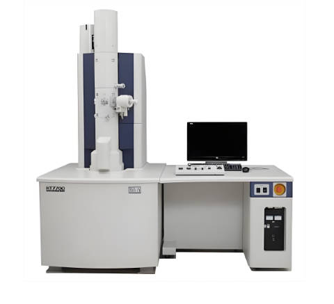
Our internationally accredited laboratory provides a specialist SEM testing service that supplies manufacturers, metallurgists, electronics producers, failure analysts, polymer scientists and materials researchers worldwide with the high‑resolution imaging and elemental microanalysis data required for quality control, process optimisation and regulatory compliance. All investigations are performed within the rigorous framework of ISO/IEC 17025, and each report bearing the ILAC mark is unconditionally accepted by regulatory authorities, customs offices and notified bodies in all major economies. The SEM testing service combines scanning electron microscopy with energy‑dispersive X‑ray spectroscopy to deliver high‑magnification topographic and compositional images, quantitative elemental analysis, line‑scan and mapping capabilities, and fracture‑surface characterisation, all at the micrometre to nanometre scale. For a steel foundry investigating casting defects, an electronics manufacturer verifying the integrity of wire bonds, or an importer screening components for RoHS compliance, our platform provides the legally robust, defensible microanalytical evidence that underpins material certification, failure‑analysis reports and international supply‑chain confidence.
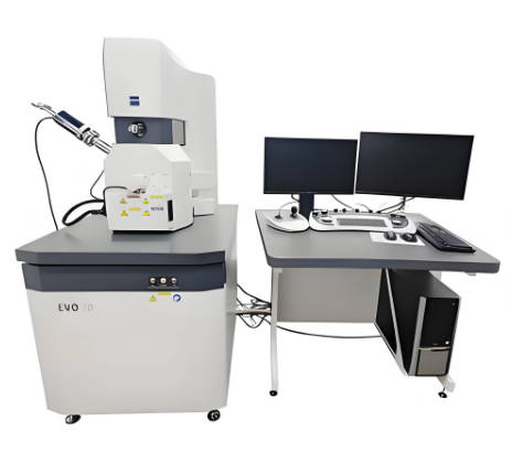
Product Samples We Regularly Subject to SEM Testing
The large‑chamber and variable‑pressure capabilities of our scanning electron microscopes accept an exceptionally wide variety of solid specimens. The following categories represent the materials most frequently analysed through our SEM testing service:
- Metals and alloys – fracture surfaces, polished cross‑sections, powder‑metallurgy compacts, steel, aluminium, titanium and nickel‑base alloy components, soldered and brazed joints
- Electronic and semiconductor devices – printed circuit boards, bond pads, wire bonds, solder bumps, lead‑frame platings, capacitor terminations and connector pins
- Ceramics, glass and refractories – sintered ceramics, glass‑to‑metal seals, thermal‑barrier coatings, furnace‑lining fragments and advanced technical ceramics
- Polymers, plastics and composites – filled thermoplastics, flame‑retardant enclosures, fibre‑reinforced laminates, rubber seals, packaging films and 3D‑printed polymer parts
- Coatings, paints and surface finishes – electroplated, anodised, PVD and CVD layers, corrosion‑resistant primers, decorative paints and conversion coatings
- Particles, residues and environmental contaminants – wear debris, airborne particulates, filter residues, corrosion products, unknown inclusions and foreign‑object debris
- Forensic, archaeological and numismatic samples – paint chips, gunshot residue, questioned documents, ancient metal artefacts and coinage alloys
- Geological and mineralogical specimens – drill‑core fragments, heavy‑mineral concentrates, micrometeorites, asbestos fibres and gemstone inclusions
High‑Resolution Imaging and Microstructural Characterisation – SEM Testing Service for Metals, Alloys and Advanced Materials
- Topographic imaging and fracture‑surface analysis according to the principles of ASTM E3 and ASTM E1508: the specimen is examined with secondary‑electron and backscattered‑electron detectors, providing three‑dimensional‑appearing images that reveal the morphology of ductile dimples, cleavage facets, fatigue striations and intergranular fracture paths. This SEM testing service enables the identification of the failure mechanism in a fractured component, directly supporting the root‑cause analysis of in‑service failures and the qualification of new materials.
- Grain‑size, phase‑distribution and inclusion‑rating assessment according to ASTM E112 and ASTM E45: polished and etched metallographic sections are imaged at calibrated magnifications, and the mean grain size, the volume fraction of second phases, and the size and number density of non‑metallic inclusions are determined by image analysis. The data are used by steel mills, foundries and forging houses to certify that the product meets the cleanliness and microstructure requirements of the purchase specification.
- Microstructural characterisation of additively manufactured alloys: the melt‑pool boundaries, the solidification cell spacing, the distribution of lack‑of‑fusion porosity and the presence of cracking in laser‑powder‑bed‑fusion or electron‑beam‑melted components are examined by SEM. The results guide the optimisation of the printing parameters and the post‑process heat treatment.
- Quantitative measurement of coating thickness and layer‑stack integrity: a cross‑section is prepared through the coating system, and the thickness of each layer – zinc, nickel, copper, tin, paint or thermal spray – is measured directly from calibrated SEM images. The uniformity, the adhesion and the presence of inter‑diffusion zones are documented, supporting the certification of electroplated, hot‑dip‑galvanized and anodised components.
- Variable‑pressure and low‑vacuum SEM for the examination of non‑conductive and outgassing specimens: uncoated polymers, ceramics, concrete, wood and biological materials are imaged in their native state without a conductive coating, preserving the surface detail and enabling the detection of cracking, fibre‑matrix debonding and filler distribution in composite materials.
Energy Dispersive X‑ray Spectroscopy (EDS/EDX) Microanalysis – Elemental Mapping and Phase Identification
- Qualitative and standardless quantitative elemental analysis according to ISO 22309 and ASTM E1508: a focused electron beam excites the sample, and the characteristic X‑ray lines of the elements from boron to uranium are detected simultaneously. The spectrum is interpreted using the ZAF or φ(ρz) matrix‑correction algorithms, and the elemental composition is reported in weight percent or atomic percent. This SEM testing service identifies unknown inclusions, corrosion products, wear debris and the composition of intermetallic phases.
- Full‑spectrum elemental mapping and line‑scan analysis: the electron beam is raster‑scanned across the field of view, and a complete X‑ray spectrum is stored at each pixel, generating quantitative elemental distribution maps. Line‑scan profiles measure the concentration gradient of each element across a weld interface, a diffusion zone, a decarburised layer or a coating‑substrate transition with sub‑micrometre spatial resolution.
- Automated particle analysis and inclusion classification: the SEM‑EDS system is programmed to scan a large representative area, automatically identify individual particles or inclusions based on their chemical contrast, and measure their size, shape and elemental composition. The number, the size distribution and the chemical class of non‑metallic inclusions in steel, filler agglomerates in a polymer or contaminant particles on a critical surface are reported.
- RoHS and hazardous‑substance screening of electronic components and consumer goods: the solders, platings, plastic housings and connector materials are analysed by EDS for the presence and concentration of lead, mercury, cadmium, hexavalent chromium and brominated flame retardants, supporting compliance with the EU RoHS Directive and the equivalent regulations of China, Japan, Korea and the Gulf States.
Failure Analysis and Contamination Investigation – Root‑Cause Problem‑Solving with SEM
- Identification of particulate contaminants and foreign‑object debris: an unknown particle, fibre or residue collected on a filter or a witness coupon is located by SEM and analysed by EDS. The elemental fingerprint is compared with a database of common contaminants, and the particle is identified as, for example, a stainless‑steel wear fragment, a brass swarf, a silica polishing residue or a PTFE fibre, enabling the source of the contamination to be traced.
- Corrosion‑product and oxidation‑layer characterisation: the elemental composition and the spatial distribution of elements within a rust scale, a tarnish film or an anodic coating are determined by point analysis and mapping. This SEM testing service identifies the aggressive species – chlorine, sulfur, alkali metals – that initiated the corrosion, and it distinguishes between protective and non‑protective oxide layers.
- Solder‑joint and micro‑interconnection integrity: the microstructure of the solder alloy, the thickness and the composition of the intermetallic‑compound layer at the pad‑solder interface, and any embrittling impurities are measured by SEM and EDS. The data support the qualification of lead‑free soldering processes, the investigation of brittle fractures in ball‑grid‑array joints and the compliance screening for the RoHS Directive.
- Reverse engineering and competitor analysis: a polished cross‑section of an unknown component – a cutting tool, a wear‑resistant coating, a multi‑layer packaging film or a decorative trim – is analysed by SEM imaging and EDS mapping. The elemental stratification, the thickness of each layer and the base‑material composition are reconstructed, providing the intelligence that product developers and patent attorneys need to assess competitive products and to protect intellectual property.
Electronics, Semiconductors and Microelectronic Devices – SEM Testing Service for Process Control and Defect Analysis
- Inspection of wire bonds, ball bonds and wedge bonds in integrated circuits: the shape, the diameter and the surface condition of the bond wire, the quality of the intermetallic formation at the bond‑pad interface, and any cracking or Kirkendall‑void formation are evaluated by SEM. The results support the qualification of the bonding process and the investigation of field‑return failures.
- Analysis of solder bumps, under‑bump metallisation and redistribution layers: the microstructure of the solder alloy, the integrity of the under‑bump metallisation stack and the presence of electromigration damage are characterised by SEM and EDS. This SEM testing service supports the development and the reliability assessment of advanced packaging technologies.
- Characterisation of printed‑circuit‑board defects – cracked vias, delamination and conductive‑anodic‑filament growth: micro‑sections through the defect are examined by SEM, and the elemental composition of the corrosion product that bridges the conductors is determined by EDS, providing the forensic evidence that guides the corrective action in the plating and etching processes.
- Measurement of thin‑film thickness and composition in semiconductor devices: a cross‑section through the gate stack, the metallisation layers or the passivation is prepared by focused‑ion‑beam milling, and the thickness and the elemental composition of each layer are measured by SEM and EDS, supporting the development and the failure analysis of advanced logic, memory and power devices.
Report Acceptance and Global Regulatory Compliance
All measurements performed within our SEM testing service are executed under the fully accredited scope of our ISO/IEC 17025 quality management system. Each test report that carries the ILAC mark is therefore automatically recognised by regulatory authorities, notified bodies, customs offices and supply‑chain partners in all major economies. For metallurgical laboratories, electronics manufacturers, failure‑analysis consultancies, polymer producers and forensic investigators anywhere in the world, the report constitutes legally robust, internationally accepted evidence that the microstructural imaging, the elemental microanalysis and the quantitative characterisation of the sample have been determined in accordance with the applicable ISO, ASTM and customer‑specified methods. The documentation can be directly used for material certification, RoHS‑compliance screening, patent‑litigation support, supplier qualification, the issue of inspection certificates according to EN 10204 or equivalent national standards, and the resolution of commercial and technical disputes concerning the microscopic structure and composition of any material.