This article provides a comprehensive overview of the testing and acceptance services required for the "New Display and Strategic Electronic Materials" key special projects. It details the critical testing standards, sample requirements, and methodologies necessary to ensure successful project completion and compliance with national research objectives.
Technical Overview
The "New Display and Strategic Electronic Materials" key special projects represent a significant focus in advanced material science research, targeting breakthroughs in display technologies and critical electronic components. As these research initiatives approach their conclusion, a rigorous testing and acceptance process is mandatory to validate that all technical indicators have been met. The completion service serves as an independent, third-party verification mechanism designed to evaluate performance, reliability, and consistency against the project's initial grant objectives.
This service ensures that the research outcomes are scientifically sound and industrially viable, facilitating the transition from laboratory prototypes to mass production. It covers a broad spectrum of materials, including flexible display substrates, semiconductor wafers, and advanced packaging materials, ensuring that every critical parameter adheres to established national and international standards.
Testing Samples
New Display Materials
The testing service accepts a variety of samples related to next-generation display technologies. These materials are critical for the development of flexible, high-resolution, and energy-efficient screens.
- OLED (Organic Light-Emitting Diode) panels and flexible substrates.
- Quantum dot (QD) films and diffusion sheets.
- Micro-LED and Mini-LED chip arrays.
- Electronic paper and electrochromic films.
Strategic Electronic Materials
This category encompasses materials vital for national infrastructure and high-end electronics manufacturing. Samples typically include:
- Third-generation semiconductors such as Silicon Carbide (SiC) and Gallium Nitride (GaN) wafers.
- Advanced packaging substrates and interconnect materials.
- High-frequency and high-speed copper-clad laminates.
- Magnetic and piezoelectric ceramic materials.
Testing Items
To verify the Key Performance Indicators (KPIs) set forth in the special project guidelines, a comprehensive range of testing items is conducted. These tests are categorized into performance validation and reliability assessment.
Performance Parameters
Performance testing focuses on the functional attributes of the materials.
- Optical Characteristics: Luminance, chromaticity coordinates, viewing angle, and contrast ratio for display panels.
- Electrical Properties: Carrier mobility, resistivity, threshold voltage, and breakdown voltage for semiconductor materials.
- Material Composition: Purity analysis, impurity concentration, and crystal structure verification.
Reliability and Environmental Stability
Reliability testing is crucial for validating the durability of materials under operational stress.
- Environmental Testing: Temperature and humidity cycling, thermal shock resistance, and UV aging tests.
- Mechanical Testing: Bending fatigue for flexible displays, peel strength for adhesive layers, and hardness testing.
- Lifespan Acceleration: High-temperature operating life (HTOL) and high-temperature storage life (HTSL) tests.
Testing Methods
All testing procedures strictly follow national standards (GB), industry-specific standards (SJ), or international protocols (IEC/JEDEC) to ensure the data is recognized by scientific and regulatory bodies. The methodology is divided into three distinct phases:
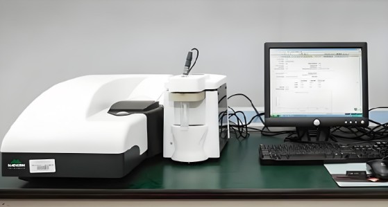
First, sample preconditioning is performed to stabilize the materials in a standard testing environment. Second, precision instrumentation such as spectrophotometers, semiconductor parameter analyzers, and scanning electron microscopes (SEM) are utilized to capture high-accuracy data. Finally, data analysis is conducted using statistical process control methods to validate the consistency of the results across multiple sample batches.
Standardization and Compliance
The service provides detailed compliance reports mapping each tested result to the specific KPIs defined in the project contract. This includes pass/fail criteria analysis and uncertainty evaluation, ensuring the results can withstand scrutiny during the formal acceptance review.
Applications
The data generated from these testing services supports a wide array of applications across the electronics industry. For new display materials, the results validate readiness for integration into consumer electronics such as smartphones, wearables, and automotive dashboards. For strategic electronic materials, the testing is essential for components used in 5G telecommunications infrastructure, power electronics for electric vehicles, and advanced aerospace systems. The successful completion of these tests paves the way for industrial scaling and commercialization.
FAQ
What is the typical duration for the completion testing service?
The duration varies depending on the complexity of the sample and the number of KPIs required. Generally, a comprehensive testing cycle, including reliability tests, takes between 15 to 30 working days.
Are the testing results accepted by national review boards?
Yes, the service is provided by accredited laboratories (CNAS/CMA certified). The reports generated are legally recognized and are a prerequisite for the formal acceptance of National Key R&D Program projects.
How should samples be prepared for submission?
Samples must be representative of the final research output. For display panels, they should be encapsulated to prevent oxidation. For semiconductor wafers, they must be shipped in cleanroom-compatible packaging to avoid contamination.