Metal Film Detection Testing Service – Accredited Thickness, Composition, Adhesion and Performance Evaluation for Global Markets
Our internationally accredited laboratory delivers a specialist metal film detection service that provides electronics manufacturers, semiconductor fabricators, optical‑coating houses, packaging converters, automotive suppliers and research institutes worldwide with the independent, traceable data they need to verify the thickness, elemental composition, microstructure, adhesion and functional performance of thin metallic layers deposited on any substrate. Every measurement is performed under the rigorous framework of ISO/IEC 17025, and each report bearing the ILAC mark is unconditionally accepted by regulatory authorities, notified bodies and supply‑chain partners in all major economies. The metal film detection programme employs a comprehensive suite of analytical and mechanical techniques – X‑ray fluorescence spectrometry, glow‑discharge optical emission spectroscopy, scanning electron microscopy with energy‑dispersive X‑ray analysis, four‑point probe resistivity measurement, spectrophotometry, cross‑cut and pull‑off adhesion testing, and environmental‑ageing chambers – to fully characterise the film and guarantee its conformance to the design specification, the industry standard and the customer’s performance requirement.
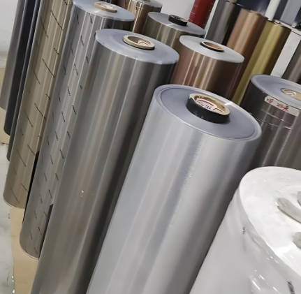
Product Samples We Regularly Subject to Metal Film Detection
The sample‑preparation and measurement capabilities in our facility accommodate metallic films on an extraordinarily diverse range of substrates. The following categories represent the most frequently tested items:
- Semiconductor and microelectronic metallisation layers – aluminium, copper, titanium, gold, platinum and tungsten films on silicon wafers, gallium arsenide and silicon‑carbide substrates, including the barrier and the seed layers
- Optical coatings and reflective films – silver, aluminium, enhanced‑aluminium and gold‑coated reflectors, dichroic filter stacks and anti‑reflection coatings on glass, polymer and ceramic substrates for the laser, the astronomical and the architectural applications
- Decorative and functional electroplated finishes – chromium, nickel, zinc, tin, brass and precious‑metal platings on steel, brass, zinc‑die‑cast and plastic components for the automotive trim, the sanitary ware and the consumer electronics
- Flexible‑packaging and barrier films – vacuum‑metallised aluminium and the transparent‑oxide‑coated polymer films for the food, the pharmaceutical and the insulation‑panel packaging
- Printed‑circuit‑board and connector contact finishes – electroless‑nickel‑immersion‑gold, hard‑gold and palladium‑nickel platings on the PCB pads and the connector pins, evaluated for the thickness, the composition and the solderability
- Thin‑film photovoltaic and energy‑device electrodes – transparent conductive oxides, molybdenum back‑contacts and silver grid‑lines on glass or flexible substrates for the solar‑cell and the battery applications
- Magnetic and data‑storage thin films – cobalt‑based and iron‑based magnetic films on the disk‑drive platters, and the magnetic‑shielding layers on the micro‑electromechanical‑system sensors
Thickness, Composition and Microstructure Analysis – Metal Film Detection According to ASTM B568, ISO 3497 and ASTM E1508
- Determination of the metallic‑film thickness by the X‑ray fluorescence spectrometry according to ASTM B568 (Standard Test Method for Measurement of Coating Thickness by X‑Ray Spectrometry) and ISO 3497 (Metallic coatings – Measurement of coating thickness – X‑ray spectrometric methods): the specimen is irradiated with a primary X‑ray beam, and the intensity of the characteristic fluorescence line of the coating metal or the substrate is measured. The thickness in micrometres or nanometres is calculated from a calibration curve, and the result is reported for the single‑layer and the multi‑layer coatings. This metal film detection method is non‑destructive, rapid and directly traceable to the national standards, and it is the primary thickness‑certification tool for the electronics and the decorative‑plating industries.
- Glow‑discharge optical emission spectroscopy for the depth‑resolved elemental composition of the multi‑layer films according to ISO 14707 (Surface chemical analysis – Glow discharge optical emission spectrometry – Introduction to use): the specimen is sputtered by a radio‑frequency glow discharge, and the emission lines of the elements are recorded as a function of the sputtering time. The quantitative depth‑profile of the coating – the thickness of each layer, the interface‑width and the inter‑diffusion of the elements – is reported, providing the definitive characterisation of the complex multi‑layer stacks.
- Scanning electron microscopy and the energy‑dispersive X‑ray spectroscopy for the surface morphology, the grain‑size analysis and the elemental mapping according to ASTM E1508 (Standard Guide for Quantitative Analysis by Energy‑Dispersive Spectroscopy): the film surface and the cross‑section are imaged at the high magnification, and the elemental composition of the selected features – the inclusions, the pits, the nodules – is identified, supporting the root‑cause analysis of the coating defects and the process optimisation.
- Coulometric and the anodic‑stripping methods for the thickness of the electroplated coatings according to ISO 2177 (Metallic coatings – Measurement of coating thickness – Coulometric method by anodic dissolution): a defined area of the coating is electrolytically dissolved, and the integrated current is converted to the thickness, providing a high‑precision reference measurement for the calibration of the X‑ray‑fluorescence instruments.
- Contact‑stylus profilometry and the optical‑interferometry for the step‑height measurement of the patterned or the etched films: the height of the step between the coated and the uncoated region is measured, and the film thickness is reported with the sub‑nanometre resolution, enabling the calibration of the deposition‑rate monitors in the sputtering and the evaporation systems.
Electrical and Optical Performance – Metal Film Detection for Conductivity, Resistivity and Reflectance
- Determination of the sheet resistance and the volume resistivity of the conductive metal films by the four‑point probe method according to ASTM F390 (Standard Test Method for Sheet Resistance of Thin Metallic Films With a Collinear Four‑Probe Array) and the semiconductor‑industry procedures: a linear array of four equally spaced probes is brought into contact with the film surface, and a known current is passed through the outer probes while the voltage drop across the inner probes is measured. The sheet resistance in ohms per square and the resistivity in ohm‑metres are calculated, providing the critical data for the conductor‑track and the electrode‑performance prediction. This metal film detection is mandatory for the incoming inspection of the indium‑tin‑oxide, the aluminium and the copper films in the flat‑panel‑display and the touch‑screen supply chain.
- Spectral reflectance and the transmittance measurement of the reflective and the semi‑transparent films according to ISO 15368 (Optics and photonics – Measurement of reflectance and transmittance) and ASTM E903: the total hemispherical reflectance and the specular transmittance are recorded over the ultraviolet, the visible and the near‑infrared regions, and the solar‑weighted reflectance and the colour coordinates are reported, certifying the optical performance of the solar‑reflector, the architectural‑glazing and the automotive‑mirror coatings.
- Eddy‑current and the magnetic‑induction thickness measurement for the non‑conductive coatings on the non‑ferrous and the ferrous substrates according to ISO 2360 (Non‑conductive coatings on non‑magnetic electrically conductive base metals – Measurement of coating thickness – Amplitude‑sensitive eddy‑current method) and ISO 2178: the thickness of the anodised‑aluminium, the paint and the polymer over‑layers on the metal films is measured, providing the complementary data for the complete coating‑system characterisation.
Adhesion, Mechanical Integrity and Wear Resistance – Metal Film Detection According to ISO 2409, ASTM D3359 and ASTM D4060
- Cross‑cut and the tape‑adhesion testing of the metal film on the rigid and the flexible substrates according to ISO 2409 (Paints and varnishes – Cross‑cut test) and ASTM D3359: a lattice pattern is scribed through the film to the substrate, a standardised pressure‑sensitive tape is applied and removed, and the area of the detached film is rated against the reference chart. The adhesion class is reported, and the test is repeated after the thermal‑cycling, the humidity‑soak and the soldering‑simulation exposures, quantifying the environmental‑durability of the bond.
- Pull‑off adhesion test according to ISO 4624 (Paints and varnishes – Pull‑off test for adhesion) and ASTM D4541: a dolly is glued to the metal‑film surface, and a tensile force is applied perpendicular to the surface until detachment occurs. The pull‑off strength in megapascals and the fracture location are reported, providing the quantitative adhesion data that the design engineer uses to guarantee the reliability of the plated component under the mechanical and the thermal loads.
- Taber‑abrasion and the falling‑sand wear testing for the durability of the decorative and the hard‑functional films according to ASTM D4060 (Standard Test Method for Abrasion Resistance of Organic Coatings by the Taber Abraser) and the internal procedures: the mass loss and the wear‑through to the substrate are measured after a defined number of the abrasion cycles, ranking the wear resistance of the chromium‑plated, the gold‑plated and the titanium‑nitride‑coated surfaces for the consumer‑product and the tooling applications.
- Micro‑hardness and the nano‑indentation testing of the thin metal films according to ISO 14577 (Metallic materials – Instrumented indentation test for hardness and materials parameters): a diamond indenter is pressed into the film surface at a controlled load, and the indentation hardness and the elastic modulus of the film alone are extracted from the load‑displacement curve, providing the intrinsic mechanical properties of the nano‑scale layer without the influence of the substrate.
Environmental Durability and Reliability – Metal Film Detection After Aging, Corrosion and Thermal Exposure
- Neutral salt‑spray and the cyclic‑corrosion testing of the electroplated and the coated components according to ISO 9227 (Corrosion tests in artificial atmospheres – Salt spray tests) and the automotive‑industry standards: the film is exposed to a continuous or a cyclic salt‑fog environment for a defined duration, and the time to the first appearance of the white or the red rust, the under‑film‑corrosion creep from the scribe and the loss of the adhesion are reported, certifying the corrosion‑protection performance of the zinc, the nickel‑chromium and the multi‑layer coatings.
- Damp‑heat and the condensing‑humidity exposure for the electronic and the optical films according to IEC 60068‑2‑78 (Environmental testing – Part 2‑78: Tests – Test Cab: Damp heat, steady state) and the internal protocols: the film is exposed to +85 °C and 85 % relative humidity for up to 1 000 hours, and the change in the electrical resistivity, the optical reflectance and the adhesion is measured, predicting the service life of the touch‑screen, the photovoltaic and the automotive‑lighting metallisations.
- Thermal‑shock and the temperature‑cycling resistance of the film‑substrate system: the specimen is rapidly transferred between a cold chamber and a hot chamber, or ramped between -40 °C and +125 °C for several hundred cycles, and the post‑cycling adhesion, the resistivity‑drift and the formation of the blisters or the cracks are evaluated, ensuring the thermo‑mechanical reliability of the coated component.
- Solderability and the wetting‑balance testing of the PCB and the connector contact finishes according to IEC 60068‑2‑54 (Environmental testing – Part 2‑54: Tests – Test Ta: Solderability testing of electronic components by the wetting balance method) and the J‑STD‑002: the time and the force of the wetting of the metal film by the molten solder are measured, providing the quantitative assurance that the gold‑plated, the palladium‑plated or the tin‑plated contact will form a reliable solder joint during the assembly.
Report Acceptance and Global Regulatory Compliance
All measurements performed within our metal film detection programme are executed under the fully accredited scope of our ISO/IEC 17025 quality management system. Each test report that carries the ILAC mark is therefore automatically recognised by regulatory authorities, notified bodies, customs offices and supply‑chain partners in all major economies. For semiconductor fabricators, electroplating‑shop operators, optical‑coating houses, printed‑circuit‑board manufacturers and consumer‑electronics assemblers anywhere in the world, the report constitutes legally robust, internationally accepted evidence that the thickness, the composition, the adhesion, the electrical and the optical performance and the environmental durability of the metal film have been determined in accordance with the applicable ASTM, ISO, IEC and customer‑specified methods. The documentation can be directly used to support the material certification, the process qualification, the issue of inspection certificates according to EN 10204 or equivalent national standards, the compilation of the technical file for the CE marking, and the resolution of commercial and technical disputes concerning the quality and the long‑term reliability of any metal‑coated product.