Energy Disperse Spectroscopy (EDS) Testing Service – Accredited Elemental Microanalysis for Global Industries
Our internationally accredited laboratory delivers a specialist Energy Disperse Spectroscopy (EDS) testing service that provides manufacturers, metallurgists, electronics producers, failure analysts, polymer scientists and materials researchers worldwide with the definitive, high‑spatial‑resolution elemental composition data they need to identify phases, verify alloy compositions, investigate surface contaminants and support root‑cause failure analysis. All analyses are performed within the strict framework of ISO/IEC 17025, and every report carrying the ILAC mark is unconditionally accepted by regulatory authorities, notified bodies and supply‑chain partners in all major economies. This Energy Disperse Spectroscopy (EDS) testing service is integrated with our scanning electron microscope platform to deliver rapid, simultaneous qualitative and quantitative elemental analysis from boron to uranium at the micron and sub‑micron scale, directly on the surface of conductive and non‑conductive materials. Whether a client needs to identify a contaminant particle on a precision bearing, map the elemental distribution across a weld interface, verify the composition of a solder joint for RoHS compliance, or reverse‑engineer a competitor's alloy, our EDS platform provides the legally robust, defensible microanalytical data that underpin product certification, process optimisation and international trade.
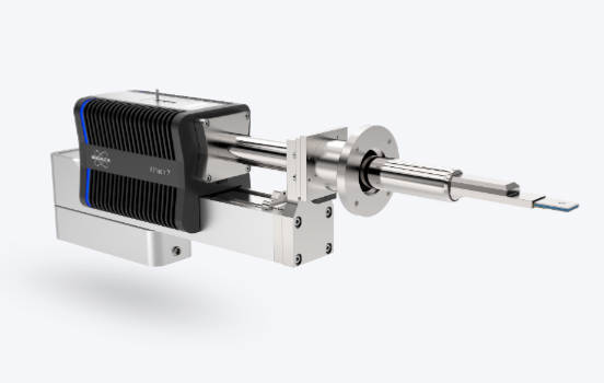
Product Samples We Regularly Analyze Using Energy Disperse Spectroscopy (EDS)
The non‑destructive, surface‑sensitive nature of our Energy Disperse Spectroscopy (EDS) testing service makes it applicable to an exceptionally wide range of solid specimens. The following categories represent the most frequently analysed items:
- Metals and alloys – fracture surfaces, polished cross‑sections, powder‑metallurgy compacts, steel, aluminium, titanium and nickel‑base alloy components, soldered and brazed joints
- Electronic and semiconductor devices – printed circuit boards, bond pads, wire bonds, solder bumps, lead‑frame platings, capacitor terminations and connector pins
- Ceramics, glass and refractories – sintered ceramics, glass‑to‑metal seals, thermal‑barrier coatings, furnace‑lining fragments and advanced technical ceramics
- Polymers, plastics and composites – filled thermoplastics, flame‑retardant enclosures, fibre‑reinforced laminates, rubber seals and packaging films
- Coatings, paints and surface finishes – electroplated, anodised, PVD and CVD layers, corrosion‑resistant primers, decorative paints and conversion coatings
- Particles, residues and environmental contaminants – wear debris, airborne particulates, filter residues, corrosion products, unknown inclusions and foreign‑object debris
- Forensic, archaeological and numismatic samples – paint chips, gunshot residue, questioned documents, ancient metal artefacts and coinage alloys
- Geological and mineralogical specimens – drill‑core fragments, heavy‑mineral concentrates, micrometeorites and gemstone inclusions
Qualitative and Quantitative Elemental Microanalysis – ISO 22309 and ASTM E1508 Standards
- Qualitative identification of elements by energy‑dispersive spectrometry: a focused electron beam excites the sample, and the characteristic X‑ray lines of the elements present are detected simultaneously. The resulting spectrum is interpreted using a digital pulse processor and advanced spectral‑mapping algorithms, and the detected elements are reported with an indication of their relative abundance. This fundamental capability of our Energy Disperse Spectroscopy (EDS) testing service rapidly identifies unknown phases, inclusions and surface contaminants without any prior knowledge of the sample composition.
- Standardless quantitative analysis according to the principles of ISO 22309 and ASTM E1508: the intensity of each element's characteristic X‑ray line is corrected for atomic‑number, absorption and fluorescence effects using the ZAF or φ(ρz) matrix‑correction algorithms. The concentrations of the detected elements are reported in weight percent or atomic percent, normalised to 100 %, with detection limits typically between 0.1 wt% and 0.5 wt% depending on the element and the matrix. This Energy Disperse Spectroscopy (EDS) testing service provides the quantitative composition of alloys, intermetallic phases, precipitates and corrosion products, and it is widely used for incoming material verification, weld‑procedure qualification and the identification of counterfeit components.
- Quantitative analysis with certified reference standards for maximum accuracy: when the highest precision is required, the EDS system is calibrated against matrix‑matched reference materials analysed under identical conditions. The elemental concentrations are reported with an expanded measurement uncertainty that includes contributions from the standard uncertainties, the counting statistics and the instrument stability, giving the client the transparent data needed for arbitration and specification compliance.
- Light‑element detection and analysis of beryllium, boron, carbon, nitrogen and oxygen: using specialised detectors with ultra‑thin polymer windows and optimised beam conditions, our EDS testing service identifies light elements that are critical for the characterisation of carbides, nitrides, oxides, borides and organic residues. The ability to detect carbon and oxygen is particularly valuable for the assessment of surface cleanliness, the identification of organic contaminants and the differentiation of oxide types on fracture surfaces.
EDS Elemental Mapping and Line Scan – Spatial Distribution of Chemical Species
- Full‑spectrum elemental mapping of microstructural features: the electron beam is raster‑scanned over a defined area, and a complete X‑ray spectrum is stored at each pixel. The resulting quantitative elemental maps reveal the distribution of each element with sub‑micron spatial resolution, showing segregation at grain boundaries, the depletion of alloying elements in the heat‑affected zone of a weld, the interdiffusion of coating constituents and the homogeneity of a powder blend. This visualisation capability of our Energy Disperse Spectroscopy (EDS) testing service is indispensable for failure analysis, process development and the characterisation of advanced multi‑phase materials.
- Line‑scan analysis across interfaces, diffusion zones and coatings: a line of equally spaced analysis points is programmed across the feature of interest, and the elemental concentration as a function of position is plotted. The technique measures the thickness and the compositional gradient of electroplated coatings, the diffusion of carbon or chromium in a carburised or nitrided case, and the width of an intermetallic layer at a solder joint or a brazed connection, providing the quantitative profile data that process engineers need to verify the effectiveness of surface treatments and joining processes.
- Phase‑area fraction and inclusion‑rating by automated feature analysis: the EDS system is programmed to scan a large representative area, identify individual particles or phases based on their chemical contrast, and measure their size, shape and composition. The volume fraction, the size distribution and the chemical classification of non‑metallic inclusions in steel, intermetallic compounds in aluminium alloys or filler agglomerates in a polymer matrix are reported, supporting the assessment of steel cleanliness, the qualification of foundry practices and the troubleshooting of compounding processes.
Failure Analysis, Contamination Investigation and Problem‑Solving with EDS
- Identification of particulate contaminants and foreign‑object debris: an unknown particle, fibre or residue is mounted on a carbon tab, located by scanning electron microscopy, and analysed by EDS. The elemental composition is compared against a database of common contaminants, and the particle is identified as, for example, a stainless‑steel wear fragment, a brass swarf, a silica polishing residue, a skin flake or a PTFE fibre. This capability of our Energy Disperse Spectroscopy (EDS) testing service enables precision‑engineering workshops, clean‑room operators and medical‑device manufacturers to trace the source of contamination and to implement effective corrective actions.
- Corrosion‑product and oxidation‑layer characterisation: the elemental composition and the spatial distribution of elements within a rust scale, a tarnish film or an anodic coating are determined by point analysis and mapping. The technique identifies the aggressive species – chlorine, sulfur, alkali metals – that initiated the corrosion, and it distinguishes between protective and non‑protective oxide layers, providing the forensic evidence that corrosion engineers use to specify the correct remedial measures.
- Solder‑joint and micro‑interconnection integrity: the composition of the solder alloy, the intermetallic‑compound layer at the pad‑solder interface and any embrittling impurities such as lead, bismuth or phosphorus are measured. This EDS testing service supports the qualification of lead‑free soldering processes, the investigation of brittle fractures in ball‑grid‑array joints and the compliance screening for the RoHS Directive, which restricts lead, mercury, cadmium and other hazardous substances in electronic equipment.
- Reverse engineering and competitor analysis: a polished cross‑section of an unknown component – a cutting tool, a wear‑resistant coating, a multi‑layer packaging film or a decorative trim – is analysed by EDS mapping and point‑quantification. The elemental stratification, the thickness of each layer and the base‑material composition are reconstructed, providing the intelligence that product developers and patent attorneys need to assess competitive products and to protect intellectual property.
Report Acceptance and Global Regulatory Compliance
All analyses performed within our Energy Disperse Spectroscopy (EDS) testing service are executed under the fully accredited scope of our ISO/IEC 17025 quality management system. Each test report that carries the ILAC mark is therefore automatically recognised by regulatory authorities, notified bodies, customs offices and supply‑chain partners in every major economy. For metallurgical laboratories, electronics manufacturers, failure‑analysis consultancies, polymer producers and forensic investigators anywhere in the world, the report constitutes legally robust, internationally accepted evidence that the micro‑elemental composition of the sample has been determined in accordance with the applicable ISO, ASTM and customer‑specified methods. The documentation can be directly used for material certification, RoHS‑compliance screening, patent‑litigation support, supplier qualification, the issue of inspection certificates according to EN 10204 or equivalent national standards, and the resolution of commercial and technical disputes concerning the elemental identity and purity of materials at the microscopic scale.