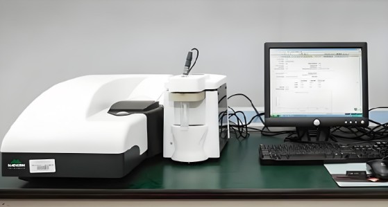
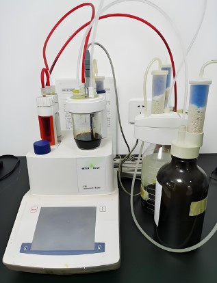
This article provides an in-depth technical analysis of the New Display and Strategic Electronic Materials Key Special Project Research Testing, highlighting critical methodologies and standards. It explores the essential testing protocols for next-generation display technologies and electronic components, offering insights into material characterization and reliability assessment.
Technical Overview
The New Display and Strategic Electronic Materials Key Special Project represents a significant initiative aimed at advancing the core technologies required for modern electronic devices. This project focuses on bridging the gap between material synthesis and commercial application through rigorous research testing. The primary objective is to validate the performance, reliability, and durability of novel materials used in displays and strategic electronic components. By establishing standardized testing frameworks, researchers can accelerate the development cycle while ensuring that materials meet the stringent requirements of industrial applications. This initiative covers a broad spectrum of materials, ranging from flexible organic light-emitting diode substrates to wide-bandgap semiconductor materials.
Testing Samples
The scope of research testing encompasses a diverse range of advanced materials categorized by their function within electronic systems. These samples serve as the foundation for empirical data collection and performance benchmarking.
Flexible Display Materials
This category includes polyimide substrates, thin-film encapsulation layers, and barrier films. These materials are critical for the development of foldable and rollable screens. Testing focuses on their mechanical flexibility, surface roughness, and optical clarity to ensure they can withstand repeated deformation without compromising display quality.
Semiconductor Wafers and Epitaxial Layers
Samples in this group include Silicon Carbide, Gallium Nitride, and Gallium Arsenide wafers. These materials are fundamental for power electronics and radio frequency devices. Testing evaluates crystalline quality, defect density, and doping uniformity to ensure high electron mobility and thermal stability.
Luminescent and Functional Films
This involves quantum dot films, organic semiconductor layers, and transparent conductive oxides like Indium Tin Oxide. The analysis focuses on photoluminescence efficiency, carrier mobility, and adhesion properties to substrate layers.
Testing Items
To comprehensively evaluate the capabilities of these materials, the project mandates a rigorous suite of testing items. These tests are designed to simulate operational conditions and identify potential failure mechanisms.
- Optical Performance Testing: Measurement of luminance, color gamut, viewing angles, and transmittance characteristics.
- Electrical Characterization: Analysis of current-voltage curves, breakdown voltage, carrier concentration, and resistivity.
- Environmental Reliability: Assessment of material stability under high temperature, high humidity, thermal cycling, and UV exposure.
- Mechanical Stress Testing: Bending tests, tensile strength analysis, and scratch resistance measurements for flexible components.
- Microstructural Analysis: Inspection of surface morphology, grain boundaries, and interface defects using high-resolution microscopy.
Testing Methods
The research employs state-of-the-art characterization techniques to ensure accurate and reproducible data. These methods provide quantitative metrics that guide material optimization and process improvements.
Spectrophotometry and Colorimetry
These techniques are utilized to quantify the optical properties of display materials. Spectrophotometers measure the reflectance and transmittance spectra, while colorimeters provide precise chromaticity coordinates. This data is essential for calibrating display performance to industry standards.
Scanning Electron Microscopy and Atomic Force Microscopy
These imaging methods are critical for analyzing the microstructure of electronic materials. They provide nanoscale resolution images of surface topography and cross-sectional structures, allowing researchers to identify pinholes, cracks, or particle contamination that could lead to device failure.
Hall Effect Measurement
This method is used to determine the electrical properties of semiconductor materials. By applying a magnetic field to a current-carrying sample, researchers can accurately measure carrier mobility, carrier concentration, and electrical conductivity, which are vital parameters for high-frequency and power devices.
Accelerated Life Testing
To predict the lifespan of materials, accelerated life testing is conducted in environmental chambers. By subjecting samples to elevated stress levels, such as extreme temperatures and voltage bias, researchers can extrapolate the operational life of the material under normal usage conditions.
Applications
The insights gained from the New Display and Strategic Electronic Materials Key Special Project have far-reaching implications across multiple high-tech industries. The validated materials enable the production of more efficient, durable, and intelligent electronic systems.
In the consumer electronics sector, the testing ensures that flexible displays used in smartphones and wearable devices maintain structural integrity and visual fidelity over thousands of folding cycles. For the automotive industry, the reliability testing of power semiconductor materials facilitates the development of efficient electric vehicle charging systems and motor drive inverters. Additionally, in the field of telecommunications, the characterization of high-frequency electronic materials supports the deployment of advanced 5G and 6G infrastructure by ensuring signal integrity and minimizing energy loss.
FAQ
This section addresses common inquiries regarding the research testing processes and objectives of the project.
What is the primary goal of this special project testing?
The primary goal is to establish a comprehensive database of material properties and failure analysis standards. This helps in reducing the time-to-market for new technologies by identifying suitable materials early in the development phase and ensuring they meet international quality standards.
How does testing improve the reliability of electronic materials?
By subjecting materials to rigorous environmental and mechanical stress tests, researchers can identify latent defects and weaknesses. This allows for the refinement of material composition and manufacturing processes, resulting in final products that are more robust and longer-lasting.
Who benefits from the outcomes of this research?
Material scientists, display manufacturers, semiconductor foundries, and end-product designers all benefit. The data generated facilitates better material selection, improved process control, and ultimately, higher quality electronic devices for consumers and industrial users.